- Europe
- Americas
- Asia and Middle East
- Africa and Oceania
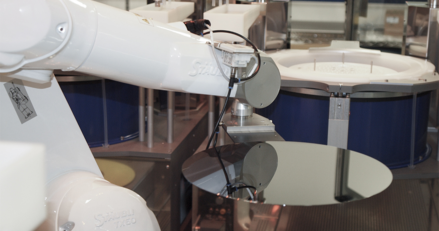
In semiconductor manufacturing, where wafer and photomask processing are critical, achieving the highest level of cleanliness, accuracy, and reliability is a must. Our robots are engineered to meet such stringent requirements
Stäubli robots are designed with a keen understanding of the need for controlled environments. They are built to minimize particle emissions—a crucial factor when any particle can have substantial implications on production yields.
For example, for mask pellicle mounting, the importance of robotic precision becomes even more pronounced. Stäubli robots are adept at performing this delicate task, their precisely controlled movements ensuring proper alignment to protect reticles for the subsequent lithography steps. Moreover, the compact footprint of these robots means that they can be integrated into the spatially constrained environments typical of cleanrooms, without sacrificing their superior performance.
In summary, robots from Stäubli provide an illustrative reference for the type of automation equipment that supports the semiconductor industry's rigorous standards.